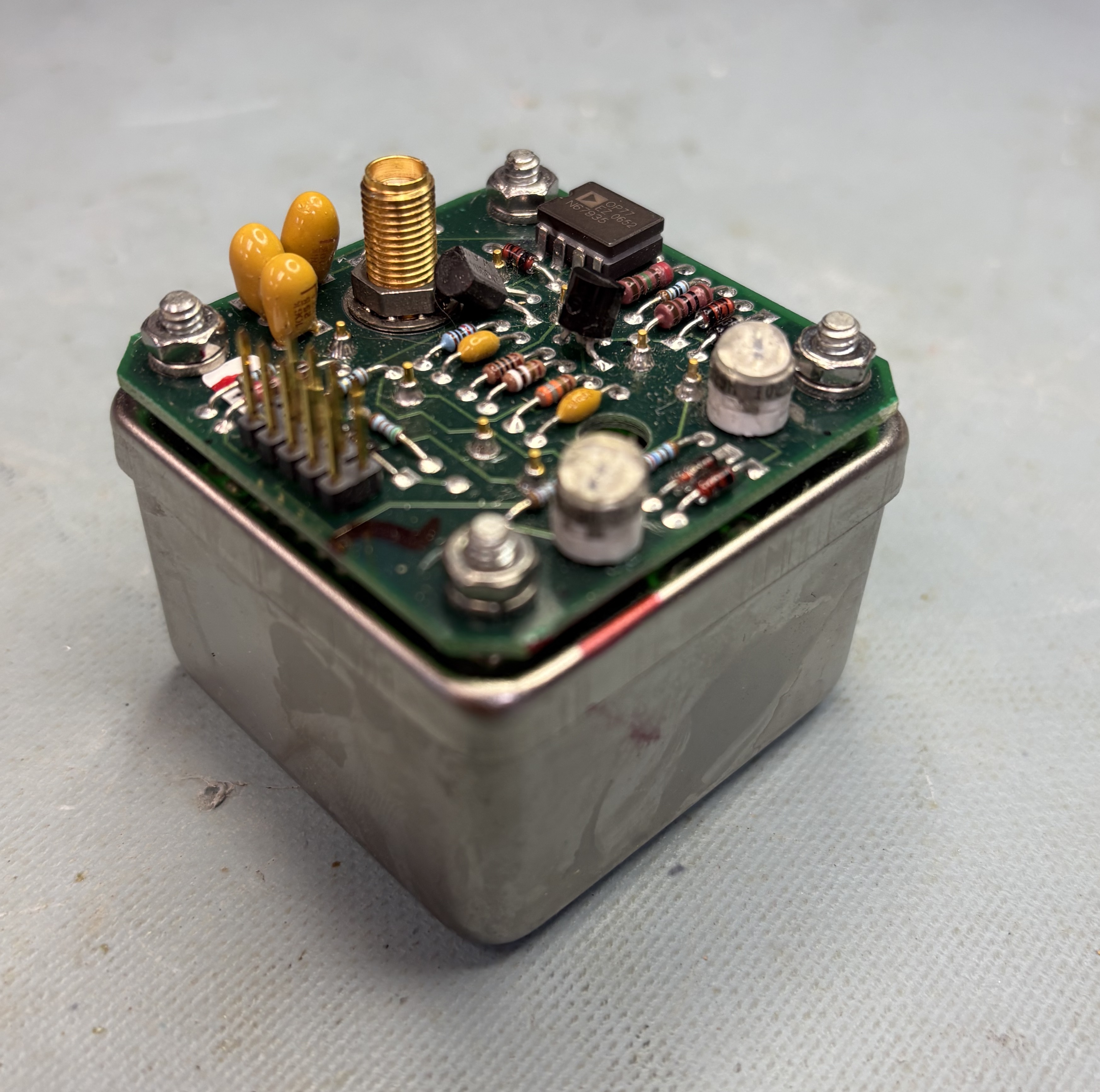
The HP 8560 series achieved its revolutionary lab-grade portability largely through two key innovations designed by the Signal Analysis Division (SAD): a highly integrated microwave front-end driven by a specialized YIG-tuned oscillator, and a deeply optimized firmware architecture packed onto internal EPROMs.
To sweep across gigahertz of frequency spectrum without producing massive internal distortions (spurious responses), SAD engineers relied on Yttrium Iron Garnet (YIG) spheres.
The creation of the YIG-Tuned Oscillator (YTO) used as the 1st Local Oscillator in the HP 8560 series spectrum analyzers is one of the most celebrated stories in microwave engineering history.
Developed by Hewlett-Packard’s Santa Rosa Division during the late 1970s and 1980s, manufacturing these oscillators required a fusion of synthetic gemstone production, precise metallurgy, and advanced micro-circuit bonding.
The complex historical engineering and manufacturing process behind the HP 8560 series YIG oscillator can be broken down into five critical stages.
The Component:
The heart of the 8560’s first local oscillator (LO) is a custom-designed, micro-sized YTO. A YIG sphere behaves like a microscopic, ultra-high-Q magnetic resonator.
Tuning Method:
By placing the sphere inside a highly precise magnetic field generated by an internal tuning coil, changing the current through the coil changes the resonant frequency linearly.
The Portability Breakthrough: Benchtop analyzers used massive, power-hungry YTOs with heavy electromagnets. SAD redesigned the YTO magnetic circuit to minimize size and power consumption so it could run coolly inside a sealed, battery-pack-friendly chassis.
1. Growing and Tumbling the YIG "Gemstones"
The heart of the oscillator is a tiny sphere of Yttrium Iron Garnet (YIG), a synthetic ferromagnetic crystal.
Crystal Pulling: HP grew single-crystal YIG ingots in high-temperature furnaces, much like silicon crystals are grown.
The Jewelry Method: The ingots were sliced into microscopic cubes. These cubes were thrown into a specialized proprietary "tumbler"—exactly like the machines used to polish rocks into smooth jewelry stones—until they formed nearly perfect spheres ranging from 10 to 30 mils (0.25 mm to 0.75 mm) in diameter.
2. Hunting for the "Anisotropy" Zero Point
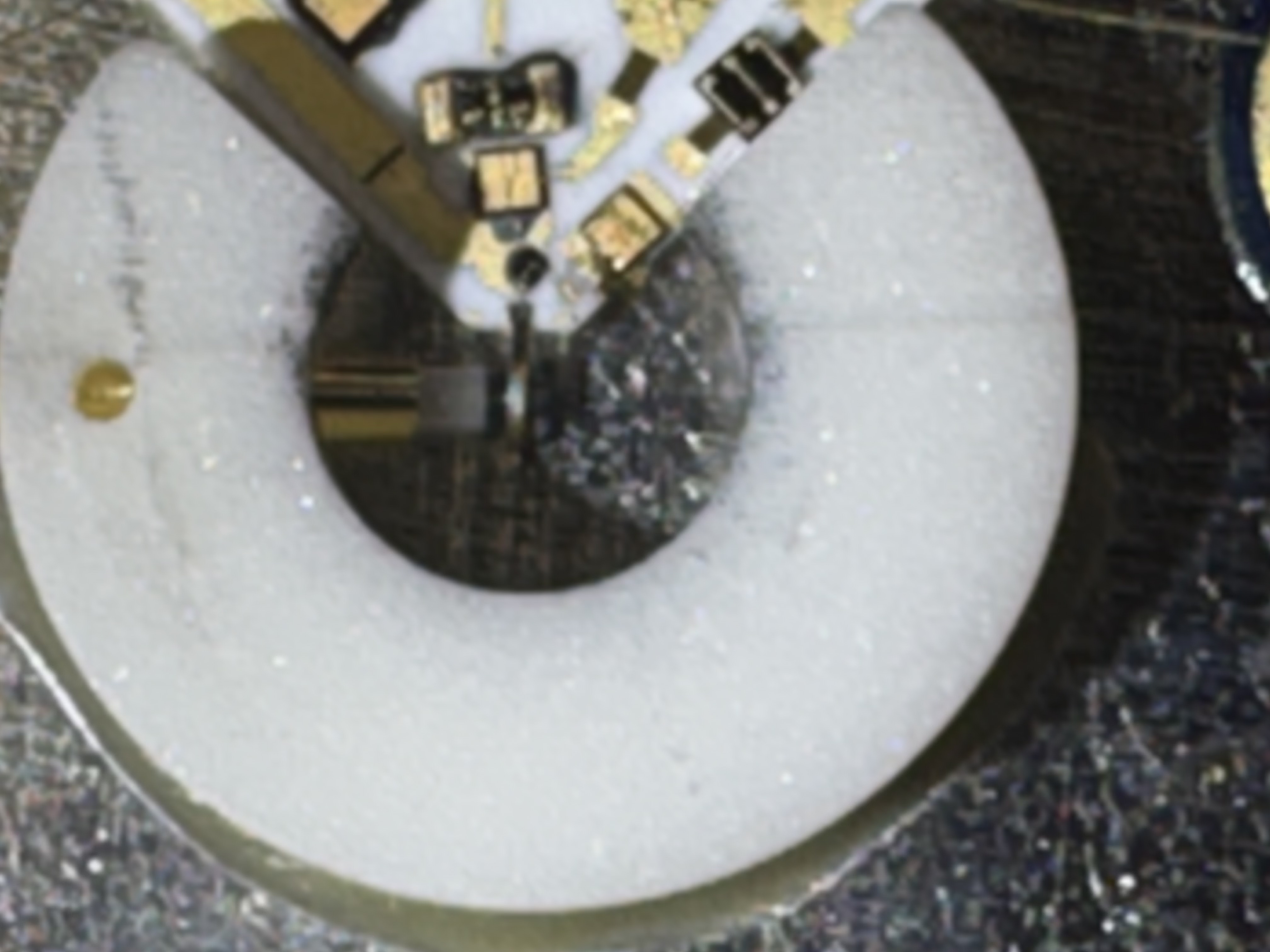
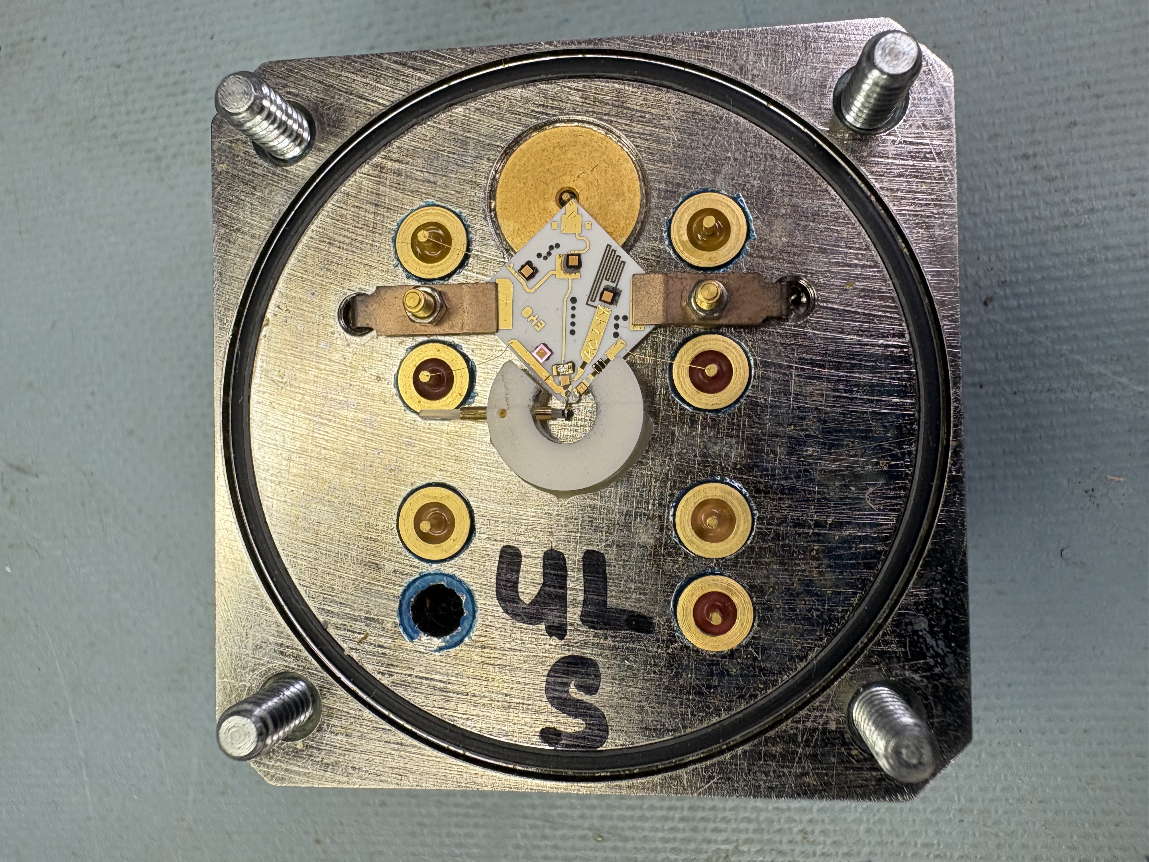
YIG crystals are highly sensitive to temperature changes, which causes frequency drift. To combat this, HP developed a meticulous alignment process:The Beryllium Oxide Rod: Technicians mounted the YIG sphere onto the tip of a rod made from Beryllium Oxide (BeO), chosen for its extreme thermal conductivity.
360-Degree Tuning: Under a microscope, engineers manually rotated the YIG sphere on the tip of the rod within a magnetic field until they found a specific Temperature Compensated (TC) axis. By locking the sphere at this precise geographic orientation, temperature-induced drift was effectively neutralized.
Micro-Heaters: The BeO rod was then outfitted with a miniature 75°C proportional heater to maintain an absolutely uniform internal temperature.
3. The 3D Coupling Loops
To inject radio frequency (RF) energy into the sphere and pull the oscillations out, HP had to construct a 3D miniature loop layout:Orthogonal Geometry: Technicians hand-soldered two tiny half-turn wire loops around the YIG sphere.
Isolation: The loops were placed at exact 90° right angles to one another. This prevented direct electromagnetic bleeding between input and output. RF energy could only pass from one loop to the other via the physical magnetic resonance (gyromagnetic precession) of the YIG sphere itself.
4. Thin-Film Micro-Circuits and Wire Bonding
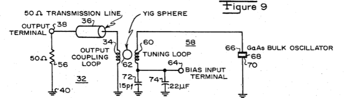
The sphere acted as the resonator, but it required a solid-state amplifier to generate the microwave signal.
Bipolar and GaAs FET Transistors: Depending on the exact generation of the 8560 oscillator (such as the early 5086-7781 or later 5086-6906), HP utilized high-frequency Silicon Bipolar or Gallium Arsenide (GaAs) FET transistors.
Gold Micro-circuitry: The components were mounted inside a gold-plated hermetic hybrid package. Technicians used microscopic gold wedge-wire bonds to connect the transistor to the YIG loops.
5. Wrapping it in a Massive Electromagnet
Because a YIG sphere's resonant frequency changes completely linearly based on magnetic field strength (2.8 MHz per Gauss), HP needed a massive magnetic engine:Main Tuning Coil: The entire micro-circuit was squeezed inside a large, heavy electromagnet utilizing massive iron pole pieces to concentrate the field directly through the YIG sphere.
This coil allowed the 8560 to cleanly sweep its Local Oscillator across its primary range (roughly 3.8 to 6.8 GHz).
FM Fine-Tuning Coil: Because the giant main coil had high inductance and tuned slowly, HP added a second, much smaller, ultra-fast "FM coil" inside the housing. This smaller coil allowed the spectrum analyzer to perform rapid phase-locking and micro-adjustments on the fly.
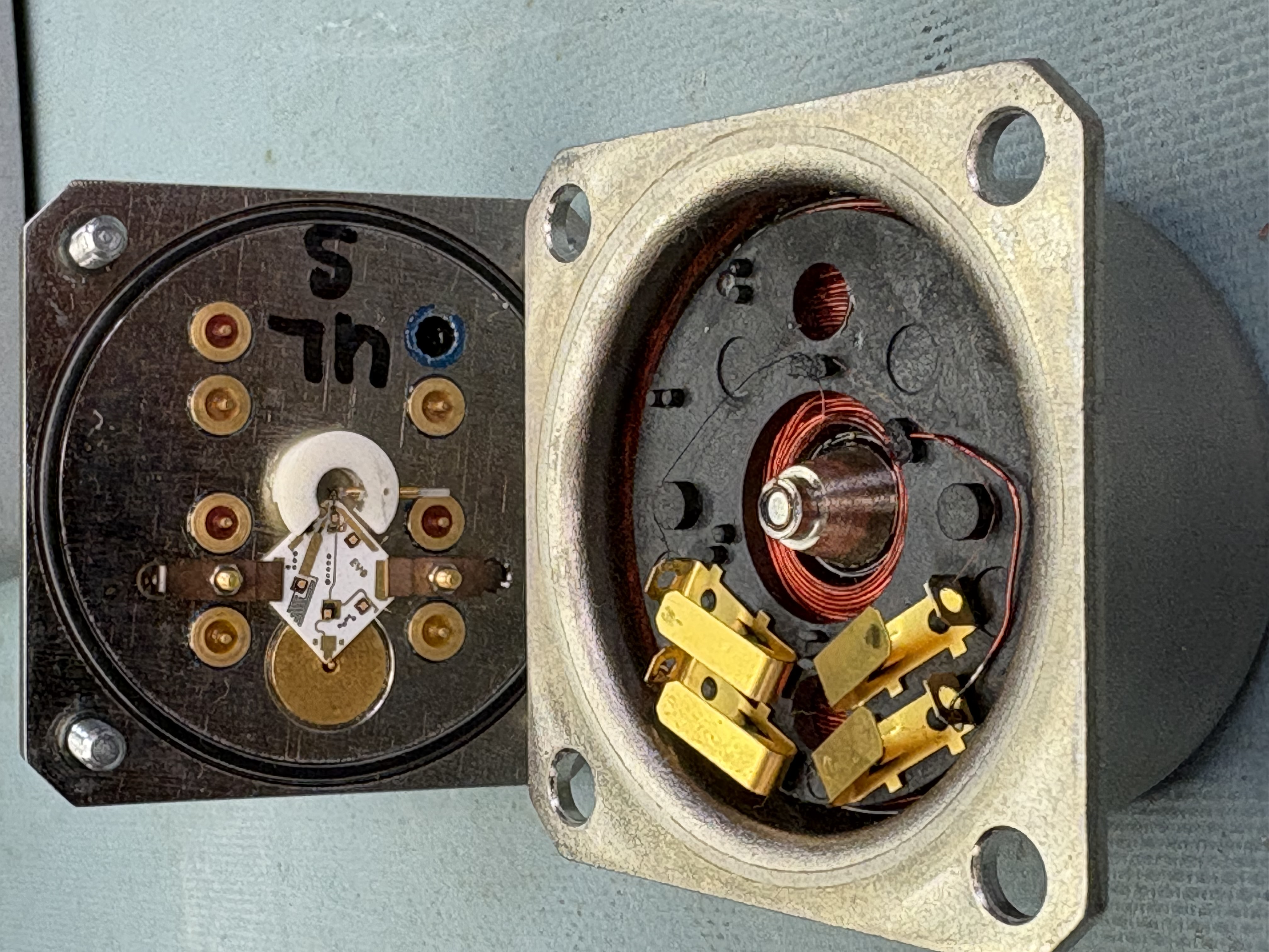
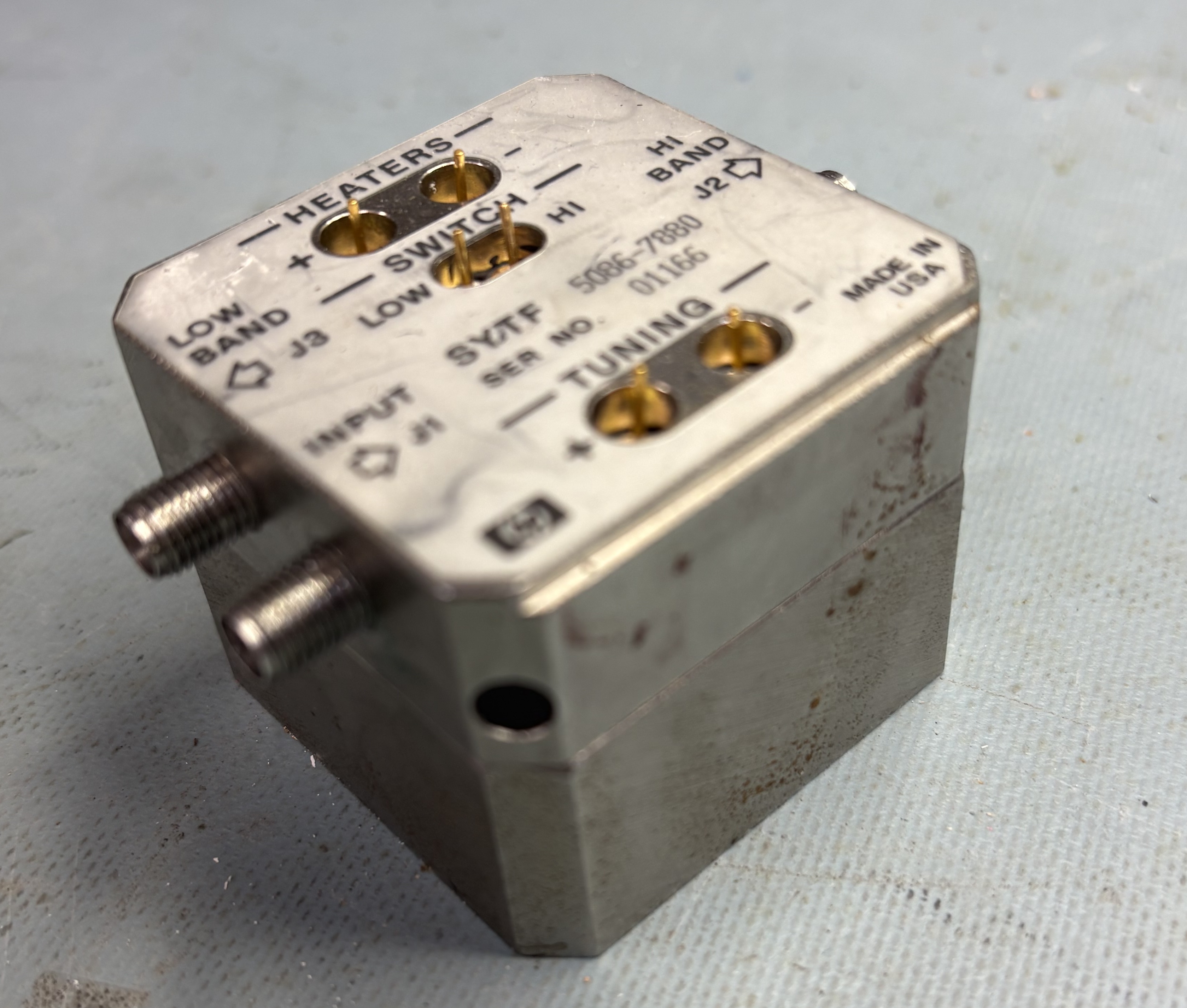
The Microwave Models (HP 8561/62/63): For models tuning above 2.9 GHz, SAD implemented a tracking YIG-Tuned Filter (YTF) directly in the RF input path.
The Purpose: When sweeping at high microwave frequencies, a harmonic mixer is used. The YTF acts as a narrow bandpass filter that tracks the exact frequency being viewed. It rejects unwanted image frequencies and powerful out-of-band signals before they hit the mixer, preventing "ghost" signals on the screen.
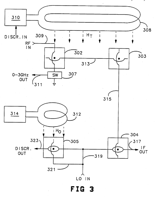
In accordance with the preferred embodiment of the present invention, four YIG-tuned resonators are combined to provide a tracking filter-mixer with a switched input. Magnetic field coils produce a magnetic tuningfield that is uniform over the four YIG resonators. The first YIG resonator acts as the first stage of the filter, and in combination with a PIN diode circuit switches the RF input signal either to the low frequency analyzer section or to the succeeding stages of the filter-mixer. The second YIG resonator acts as the second stage of the filter. The third YIG resonator acts as the third stage of the filter, and as a fundamental mixer for combining the RF input signal with a swept LO signal to
The firmware of the HP 8560 series handles everything from digital control of the hardware loops to calculating fast Fourier transforms (FFTs) and parsing HP-IB (GPIB) programming language.
The series utilizes a primary Motorola 68000-family microprocessor paired with a custom digital ASIC (Application-Specific Integrated Circuit) to control the display sweeps and fast data acquisition.
Storage: The operating code is stored entirely on physical, socketed UV-erasable EPROMs (typically 27C512 or similar chips) located on the A2 controller board.
The firmware evolved dramatically from the original 1989 launch through the late-1990s E-series lifecycle:Early Firmware (Pre-1992 / Rev 89xxxx to 91xxxx): Focus was entirely on pure instrument control, managing the tight Fractional-N synthesizer lock routines, and standard analog CRT vector-drawing routines.
The 1993 Digital Processing Leap (Rev 93xxxx and later): With the introduction of the E-series, firmware rewrites allowed for true Digital Resolution Bandwidths (RBW) down to 1 Hz, 3 Hz, and 10 Hz. The firmware processes these narrow sweeps using digital filtering algorithms rather than waiting for analog circuits to settle, vastly speeding up slow microwave sweeps.
Mass Storage & Custom App Personalities: Later firmware revisions introduced code to support internal memory cards. Technicians could plug in a physical ROM card containing specific software "personalities" (such as GSM, phase noise testing, or cable TV measurements). The firmware dynamically loaded these sub-menus directly into the user interface.
The Calibration Matrix
Because YIG oscillators alter their frequency response slightly based on ambient temperature, the firmware stores a dense, factory-generated calibration error correction matrix in non-volatile RAM (NVRAM). During the instrument's automatic boot-up and periodic background "Cal Clean" routines, the firmware measures internal drift against a built-in 300 MHz reference signal and adjusts the YTO drive currents in real time to maintain flawless accuracy.