your analyzer repair facility

We specialize in the Repair and Calibr​​ation of ​Obs​​olete & No Longer Supported Spectrum and Netw​​ork Analyzers

DC-67GHz 

HP 8560 Series Spectrum Analyzers:
 
Technical History & Repair

The History & Development of Portable Microwave Performance

Prior to the late 1980s, engineers requiring high dynamic range, low phase noise, and synthesized tuning had to rely on monolithic lab benches like the HP 8566A/B. However, these systems weighed over 110 lbs.

To solve this, HP developed the 8560 series architecture to package true laboratory-grade performance into a compact footprint weighing roughly 40 lbs.

The Core Innovation:

HP downsized complex YIG-tuned oscillators (YTO) and multi-stage inte​rmediate frequency (IF) sections into a modular, ruggedized enclosure.

MIL-Rugged Standards:

The series was designed to meet strict MIL-T-28800C Class 3 requirements. This guaranteed protection against heavy shock, rapid transit drops, and extreme field temperatures (-10°C to +55°C).

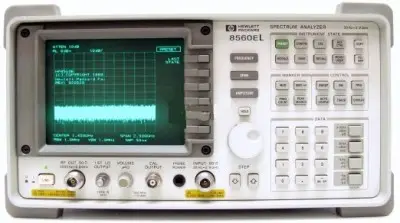
The HP 8560X Series (commonly referenced as the HP 8560 series) is a legendary family of high-performance, portable spectrum analyzers. Introduced by Hewlett-Packard (later Agilent, now Keysight Technologies), they served as the gold standard for Radio Frequency (RF) and microwave analysis for decades. They bridge the gap between heavy, stationary benchtop equipment and low-performance field units

Evolution of the 8560 Generations


The architecture evolved across three major generations, primarily distinguished by processing speed and display technologies:

Feature / Generation

A/B Series (Late 1980s)

E-Series (1990s)

EC-Series (Early 2000s)

Primary Display

Monochrome CRT (Green Vector)

Monochrome CRT (Improved Resolution)

Bright Color LCD Screen

Minimum RBW

10 Hz

1 Hz (Digital Filter)

1Hz

Sweep Speeds

Standard analog sweep

Optional Fast ADC (Option 007)

Standard Fast ADC (down to 50 µs)

Video Output

None standard

None standard

Built-in VGA Port


The HP 8560 Series spectrum analyzers were designed and built by  Hewlett-Packard's Signal Analysis Division (SAD)  located at 1400 Fountaingrove Parkway in Santa Rosa, California.

Introduced in the late 1980s (beginning with the HP 8562A and followed by the 8560A, 8561B, and 8563A), this iconic family of instruments transitioned HP's high-performance microwave analysis from massive benchtop units into a highly rugged, portable form factor.

The creation of the 8560 series relied on a sophisticated "team of teams" engineering approach, leveraging specialized cross-functional groups under HP's classic matrix management system.


The Cross-Functional Engineering Teams Behind the Design

Developing a portable microwave spectrum analyzer required shrinking advanced technologies previously reserved for multi-box setups—like the legendary 112 lb HP 8566A/B—into a 40 lb package. 

The engineering organization was segmented into several highly coordinated teams:

1. The RF & Microwave Hardware Team

This team was responsible for the critical high-frequency front end. Their primary challenge was minimizing distortion, expanding dynamic range, and maintaining incredible sensitivity (down to -130 dBm) within a confined, tightly shielded space.

  • YIG and Filter Design: They closely collaborated with HP's in-house microelectronics components groups to design customized Yig-Tuned Oscillators (YTOs) and Yig-Tuned Filters (YTF).
  • The Input Mixer Group: They developed high-frequency, low-loss input mixers capable of sweeping cleanly across extreme frequency bands (up to 26.5 GHz for the 8563A, and out to millimeter-wave using external mixers).

2. The Synthesizer & Phase-Lock-Loop (PLL) Team

The 8560 series was heavily marketed for its synthesized tuning accuracy.

The Local Oscillator (LO) Challenge: The core of a high-performance spectrum analyzer is its first LO. This team engineered a specialized sweeping synthesizer using complex multi-loop phase-locked topologies to achieve exceptionally low phase noise and precise fractional-N frequency synthesis. Their design ensured that when you tuned to a frequency, it stayed perfectly locked without drifting.

3. The Digital Intermediate Frequency (IF) & Signal Processing Team

As the analog signal was down-converted, it passed into the IF section.

Bandwidth Selectivity: This group designed the discrete LC, crystal, and digital resolution bandwidth (RBW) filters (ranging down to 10 Hz, 30 Hz, and 100 Hz).
Log Amplifiers and ADCs: They engineered the high-accuracy logarithmic amplifiers that converted analog power levels into the decibel scales displayed on the CRT screen.

4. The Digital Hardware & Firmware Team

Spectrum analyzers of this era were transitioning into full microprocessor control. 

  • The Embedded Architecture: This team designed the motherboard around Motorola 68000-series microprocessors, which handled front-panel inputs, automated calibrations (IF ADJ routines), and managed data conversion for display on the CRT.
  • Firmware: Written primarily in highly optimized assembly and procedural languages, the firmware team developed the instrument's firmware architecture, remote HP-IB / GPIB programming commands, and early on-screen menus.

5. Mechanical & Environmental Packaging Team

To achieve the MIL-T-28800C ruggedization standard, a highly specialized mechanical team was assigned to design the physical enclosure.

  • Thermal Management: Portable instruments have tight spaces that trap heat, which degrades high-frequency component stability. This team designed extensive internal casting, heat sinking, and airflow pathways to keep the microwave components within a strict temperature margin.
  • RFI/EMI Shielding: Because an analyzer measures microscopic RF signals, it cannot allow leakage from its own internal digital microprocessors to bleed into the analog front end. The mechanical team developed heavy, compartmentalized aluminum die-cast housings (clamshell modules) to shield each section.

Manufacturing Innovation at the Santa Rosa Facility

The making of the HP 8560 Series spectrum analyzers at the Hewlett-Packard Santa Rosa Facility (located at 1400 Fountaingrove Parkway, CA) represents a masterclass in combining advanced microwave microcircuitry with high-volume, military-grade ruggedized manufacturing.
The production line at Santa Rosa utilized a highly integrated process, bridging cutting-edge semiconductor fabrication with rugged component packaging.


1. In-House Microcircuit Fabrication (MWTC)

The heart of the HP 8560 series relied on components that could not be purchased from third-party vendors. They were built from scratch at Santa Rosa's on-site Microwave Technology Center (MWTC):
YIG Oscillator Production: Santa Rosa technicians grew and polished Yttrium Iron Garnet (YIG) spheres. These spheres served as the core of the high-frequency first Local Oscillator (LO), delivering highly stable synthesized tuning.

Thin-Film Hybrid Circuits:

Technicians used photolithography to deposit precise gold circuitry onto sapphire and ceramic substrates. These substrates housed the analyzer’s critical front-end mixers, step attenuators, and switch matrices.

GaAs Semiconductor Lab:

The facility fabricated custom Gallium Arsenide (GaAs) field-effect transistors (FETs) and high-frequency diodes to manage the 50 Hz to 26.5 GHz (and higher) frequency ranges natively handled by the 8560 series.

2. High-Density Mechanical Packaging

To make the 8560 series portable yet extremely durable, HP engineers designed a specialized internal cast-aluminum chassis layout:Modular Hinged Layout: The internal architecture was built on a series of sandwich-style hinged aluminum frames. The A2 Controller, A3 Interface, A4 Top Sweep, and A5 IF assemblies folded out like pages in a book. This allowed for incredibly dense packaging while keeping the instrument repairable.
Inter-assembly Isolation: The aluminum frames doubled as deep-groove shielding cavities. When folded closed, the cavities prevented RF leaks between the sensitive Intermediate Frequency (IF) processing stages and the digital processor boards.

3. Environmental and MIL-SPEC Testing

Because the HP 8560 series was engineered for field service and military deployment, completed units underwent rigorous environmental stress screening (ESS) at Santa Rosa:Shock and Drop Stations: Units were subjected to pneumatic pulse-shock tests up to 30 g's of force to simulate transit drops and harsh field conditions.
Environmental Chambers: Assembled units were baked and frozen in environmental chambers to ensure they met full calibration specifications throughout a -10°C to +55°C temperature range.
The 5-Minute Warm-Up Standard: The manufacturing team tuned the internal ovens of the reference oscillators so precisely that the instruments could achieve rock-solid, fully calibrated frequency accuracy within exactly five minutes of a cold start.

4. Automated Software Calibration

Once an analyzer passed physical inspections, it was paired with an automated factory test system running HP Basic software on local workstations.EEROM Characterization: The system mapped the subtle non-linearities of the custom input mixers and attenuators. It stored these correction factors directly onto the instrument's internal Electrically Erasable Programmable Read-Only Memory (EEROM).
Traceability: This automated calibration step ensured every shipped unit was perfectly linear and traceable directly to the National Institute of Standards and Technology (NIST).

Key Inventions & Components Produced:

The Planar Doped Barrier (PDB) Diode: This was HP’s secret weapon for the 8560 series input mixer. Traditional Schottky diodes suffered from high noise and fragile power handling. The Santa Rosa Fab used Molecular Beam Epitaxy (MBE) to grow GaAs wafers layer by single-atom layer. They engineered a microscopic "bulk" barrier inside the semiconductor material itself. The resulting PDB diodes gave the 8560 series an incredibly flat frequency response and ruggedness against accidental front-panel RF overloads.

GaAs MMICs (Monolithic Microwave Integrated Circuits): The lab fabricated custom GaAs FETs (Field Effect Transistors) and traveling-wave amplifiers. By integrating capacitors, resistors, and transistors onto a single GaAs die, they drastically shrank the physical size of the internal gain blocks, allowing the 8560 series to remain portable.

Disclaimer
The information provided on this page regarding the design, engineering history, and manufacturing processes of the HP 8560 series spectrum analyzers is for educational and historical informational purposes only. "HP," "Hewlett-Packard," "Agilent," and "Keysight" are registered trademarks of their respective owners. This content is an independent historical overview and is not affiliated with, endorsed by, or officially connected to Keysight Technologies or any of its subsidiaries. While every effort has been made to ensure historical and technical accuracy based on publicly available documentation, retro-engineering community insights, and historical archives, all technical specifications, internal architectures, and division names are subject to change or correction. The author assumes no liability for any errors, omissions, or damages resulting from the use or interpretation of this information.