your analyzer repair facility

We specialize in the Repair and Calibr​​ation of ​Obs​​olete & No Longer Supported Spectrum and Netw​​ork Analyzers

DC-67GHz 

YIG-tuned oscillator and firmware architecture

The HP 8560 series achieved its revolutionary lab-grade portability largely through two key innovations designed by the Signal Analysis Division (SAD): a highly integrated microwave front-end driven by a specialized YIG-tuned oscillator, and a deeply optimized firmware architecture packed onto internal EPROMs.

1. The Microwave Front-End & YIG Technology

To sweep across gigahertz of frequency spectrum without producing massive internal distortions (spurious responses), SAD engineers relied on Yttrium Iron Garnet (YIG) spheres.

The YIG-Tuned Oscillator (YTO)

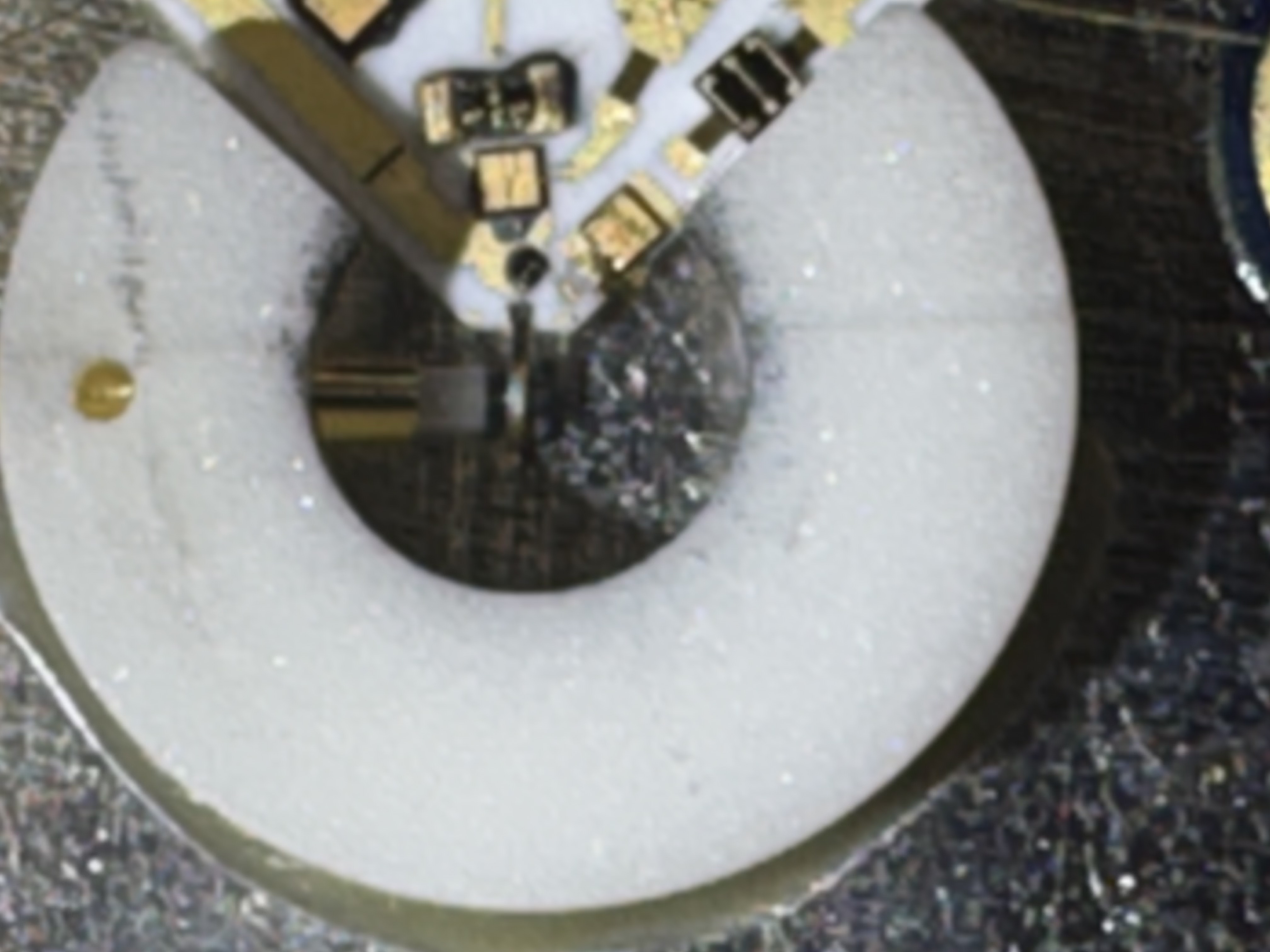
The creation of the YIG-Tuned Oscillator (YTO) used as the 1st Local Oscillator in the HP 8560 series spectrum analyzers is one of the most celebrated stories in microwave engineering history. Developed by Hewlett-Packard’s Santa Rosa Division during the late 1970s and 1980s, manufacturing these oscillators required a fusion of synthetic gemstone production, precise metallurgy, and advanced micro-circuit bonding. The complex historical engineering and manufacturing process behind the HP 8560 series YIG oscillator can be broken down into five critical stages.

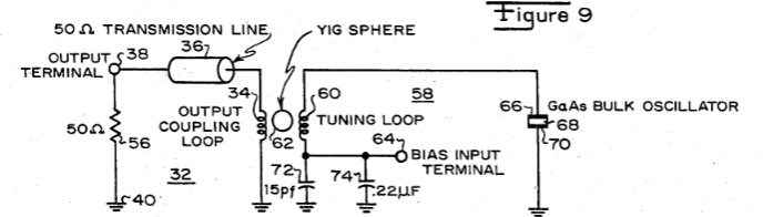
The Component: The heart of the 8560’s first local oscillator (LO) is a custom-designed, micro-sized YTO. A YIG sphere behaves like a microscopic, ultra-high-Q magnetic resonator.

Tuning Method: By placing the sphere inside a highly precise magnetic field generated by an internal tuning coil, changing the current through the coil changes the resonant frequency linearly.

The Portability Breakthrough: Benchtop analyzers used massive, power-hungry YTOs with heavy electromagnets. SAD redesigned the YTO magnetic circuit to minimize size and power consumption so it could run coolly inside a sealed, battery-pack-friendly chassis.

1. Growing and Tumbling the YIG "Gemstones"

The heart of the oscillator is a tiny sphere of Yttrium Iron Garnet (YIG), a synthetic ferromagnetic crystal.

  • Crystal Pulling: HP grew single-crystal YIG ingots in high-temperature furnaces, much like silicon crystals are grown.
  • The Jewelry Method: The ingots were sliced into microscopic cubes. These cubes were thrown into a specialized proprietary "tumbler"—exactly like the machines used to polish rocks into smooth jewelry stones—until they formed nearly perfect spheres ranging from 10 to 30 mils (0.25 mm to 0.75 mm) in diameter.

2. Hunting for the "Anisotropy" Zero Point

YIG crystals are highly sensitive to temperature changes, which causes frequency drift. To combat this, HP developed a meticulous alignment process:

  • The Beryllium Oxide Rod: Technicians mounted the YIG sphere onto the tip of a rod made from Beryllium Oxide (BeO), chosen for its extreme thermal conductivity.
  • 360-Degree Tuning: Under a microscope, engineers manually rotated the YIG sphere on the tip of the rod within a magnetic field until they found a specific Temperature Compensated (TC) axis. By locking the sphere at this precise geographic orientation, temperature-induced drift was effectively neutralized.
  • Micro-Heaters: The BeO rod was then outfitted with a miniature 75°C proportional heater to maintain an absolutely uniform internal temperature.

3. The 3D Coupling Loops

To inject radio frequency (RF) energy into the sphere and pull the oscillations out, HP had to construct a 3D miniature loop layout:

  • Orthogonal Geometry: Technicians hand-soldered two tiny half-turn wire loops around the YIG sphere.
  • Isolation: The loops were placed at exact 90° right angles to one another. This prevented direct electromagnetic bleeding between input and output. RF energy could only pass from one loop to the other via the physical magnetic resonance (gyromagnetic precession) of the YIG sphere itself.

4. Thin-Film Micro-Circuits and Wire Bonding

The sphere acted as the resonator, but it required a solid-state amplifier to generate the microwave signal.

  • Bipolar and GaAs FET Transistors: Depending on the exact generation of the 8560 oscillator (such as the early 5086-7781 or later 5086-6906), HP utilized high-frequency Silicon Bipolar or Gallium Arsenide (GaAs) FET transistors.
  • Gold Micro-circuitry: The components were mounted inside a gold-plated hermetic hybrid package. Technicians used microscopic gold wedge-wire bonds to connect the transistor to the YIG loops.

5. Wrapping it in a Massive Electromagnet

Because a YIG sphere's resonant frequency changes completely linearly based on magnetic field strength (2.8 MHz per Gauss), HP needed a massive magnetic engine:

  • Main Tuning Coil: The entire micro-circuit was squeezed inside a large, heavy electromagnet utilizing massive iron pole pieces to concentrate the field directly through the YIG sphere. This coil allowed the 8560 to cleanly sweep its Local Oscillator across its primary range (roughly 3.8 to 6.8 GHz).
  • FM Fine-Tuning Coil: Because the giant main coil had high inductance and tuned slowly, HP added a second, much smaller, ultra-fast "FM coil" inside the housing. This smaller coil allowed the spectrum analyzer to perform rapid phase-locking and micro-adjustments on the fly.

Low-Level Architecture of Pre-1992 Firmware

Early firmware (revisions 89xxxx to 91xxxx) operated as a bare-metal controller. It lacked a modern operating system layer, directly mapping execution loops to processor interrupts.

Fractional-N Synthesizer Lock Routines

  • Phase Accumulator Management: The firmware calculated precise frequency steps by constantly reloading phase accumulator registers. It managed fractional division ratios to prevent integer boundary spurs.
  • Settling Loop Timing: Firmware routines monitored analog phase detector voltage windows. It implemented hardcoded timing delays to ensure the local oscillator (LO) stabilized before sampling RF energy.
  • Phase Noise Compensation: Early code executed active look-up tables to apply correction voltages to the voltage-controlled oscillator (VCO). This counteracted inherent phase noise during fast frequency hops.

Analog CRT Vector-Drawing Architecture

  • X-Y Deflection Control: The firmware translated frequency (X-axis) and amplitude (Y-axis) data into precise voltage steps for digital-to-analog converters (DACs). These DACs directly drove the horizontal and vertical CRT deflection plates.
  • Blanking Vector Logic: Specialized interrupt routines handled the CRT electron gun blanking. This turned off the beam during retrace periods to prevent ghost lines across the display screen.
  • Refresh Rate Syncing: Code execution loops were strictly synchronized with the mains power frequency (50/60 Hz). This minimized visible screen flicker and display jitter caused by magnetic stray fields.

The 1993 Digital Processing Leap (Rev 93xxxx+)

The transition to E-series instruments shifted narrow-bandwidth filtering from analog LC circuits and crystal filters to real-time digital computation.

 +----------------------------------------------+
                  |            1993 DSP FIRMWARE PATH            |
                  |                                              |
[Analog IF Mixer]---> [ADC] ---> [Digital Down-Converter]        |
                  |                        |                     |
                  |                        v                     |
                  |               [Decimation Filters]           |
                  |                        |                     |
                  |                        v                     |
                  |              [Windowing & FFT/FIR] --------> [Display Math]
                  +----------------------------------------------+ 

Software-Driven Digital Resolution Bandwidths

  • Decimation and Filtering Loops: The firmware down-converted the intermediate frequency (IF) and passed it through multi-stage decimation filters. This isolated narrow frequency chunks without relying on large, temperature-sensitive analog components.
  • FIR/IIR Algorithm Implementation: Firmware engineers coded Finite Impulse Response (FIR) and Infinite Impulse Response (IIR) filters directly into machine code. These simulated near-perfect Gaussian filter shapes mathematically.
  • Bypassing Analog Settling Delays: Analog 1 Hz filters require seconds or minutes to settle due to high quality-factor (Q) energy storage. The 1993 firmware bypassed this by processing data using fast math equations, cutting sweep times down significantly.

Mass Storage & UI Extensibility (Late 1990s)

The late-1990s architecture turned a fixed-function hardware box into a modular software platform using external ROM cards.

Dynamic Memory Allocation

  • Memory Bank Switching: The system microprocessor used hardware bank-switching to map external ROM card addresses directly into the instrument's main CPU memory space.
  • Interface Overlays: Application personalities contained binary UI descriptions. When inserted, the primary firmware parsed these files to inject custom softkeys and menus into the native display tree.
  • Vector Object Merging: The core drawing engine merged standard trace graphics with custom measurement lines (e.g., GSM limit lines or Cable TV channel grids) loaded directly from the card.

Specialized Measurement Personalities

  • GSM Validation: Automated routines calculated phase error, burst timing, and power-versus-time profiles against strict cellular standards.
  • Phase Noise Testing: Firmware automated the log-frequency sweep, calculated carrier power offsets, and plotted single-sideband (SSB) phase noise curves directly.
  • Cable TV (CATV) Diagnostics: Code modules added dedicated testing functions for carrier-to-noise ratios (C/N), hum modulation, and discrete channel frequency logging.

The YIG-Tuned Filter (YTF) / Preselector

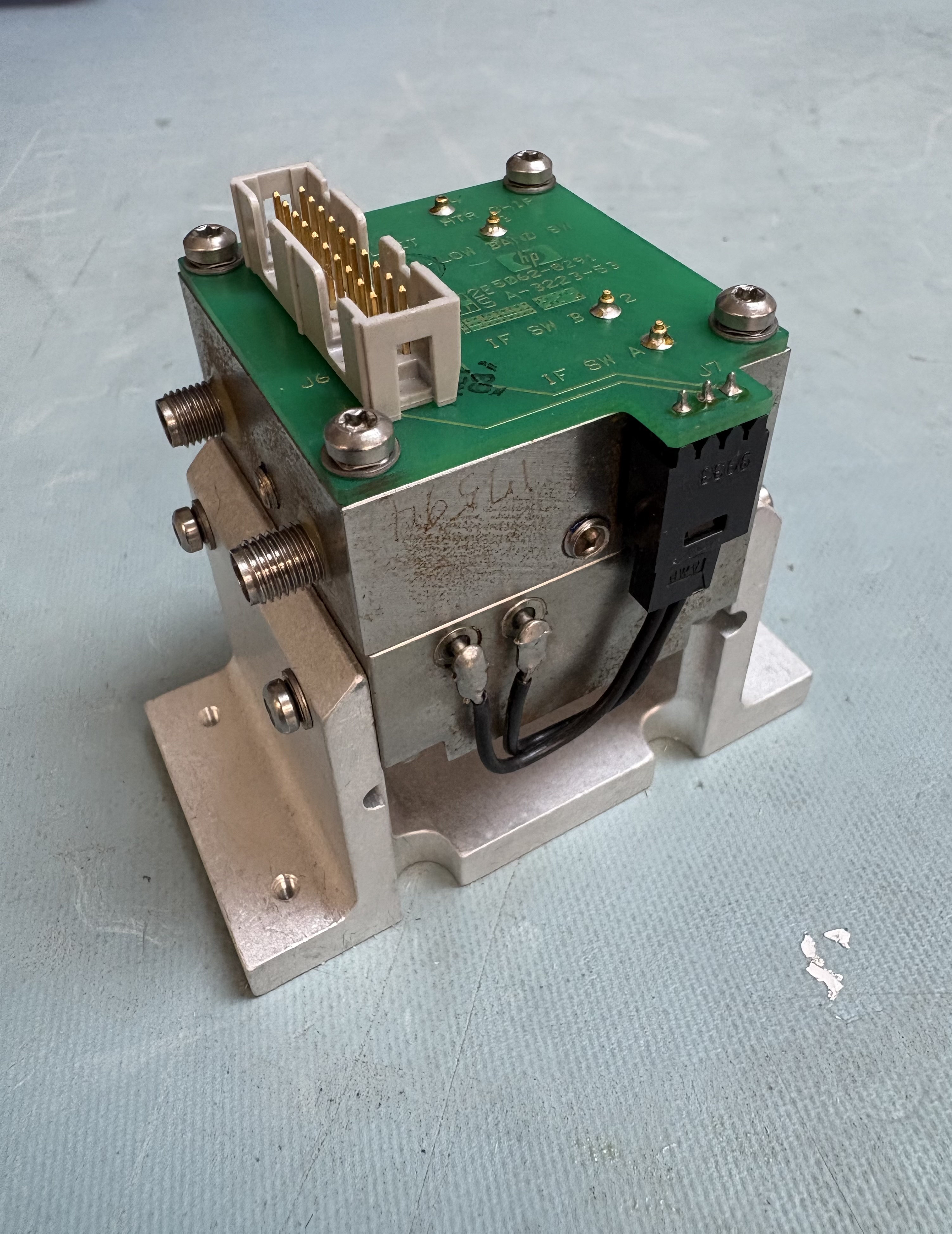
The Microwave Models (HP 8561/62/63): For models tuning above 2.9 GHz, SAD implemented a tracking YIG-Tuned Filter (YTF) directly in the RF input path.

The Purpose: When sweeping at high microwave frequencies, a harmonic mixer is used. The YTF acts as a narrow bandpass filter that tracks the exact frequency being viewed. It rejects unwanted image frequencies and powerful out-of-band signals before they hit the mixer, preventing "ghost" signals on the screen.

Four-Resonator Tracking Filter-Mixer Architecture

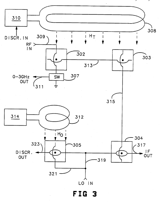
In accordance with the preferred embodiment of the present invention, four YIG-tuned resonators are combined to provide a tracking filter-mixer with a switched input. Magnetic field coils produce a magnetic tuning field that is uniform over the four YIG resonators.

  • The First YIG Resonator: This resonator acts as the first stage of the filter, and in combination with a PIN diode circuit switches the RF input signal either to the low frequency analyzer section or to the succeeding stages of the filter-mixer.
  • The Second YIG Resonator: This resonator acts as the second stage of the filter.
  • The Third YIG Resonator: This resonator acts as the third stage of the filter, and as a fundamental mixer for combining the RF input signal with a swept LO signal.

Key Milestones in the Firmware Evolution

This historical evolution highlights a classic shift in RF test equipment from hardware-dependent instruments to software-defined architectures. The transition from managing physical analog limitations to executing digital signal processing (DSP) algorithms completely redefined spectrum analyzer performance in the 1990s.

  • Pre-1992 (Foundational Control): Firmware was highly specialized, focusing on low-level tasks like synthesizer lock routines and managing analog CRT deflection coils.
  • 1993 (The DSP Leap): Software algorithms replaced analog components to enable narrow Resolution Bandwidths (RBW) down to 1 Hz. This drastically reduced sweep times for tight spans by eliminating analog settling delays.
  • Late-1990s (Extensibility): Instruments shifted toward platform-based architectures by supporting memory cards. This allowed field updates and specialized firmware "personalities" (e.g., GSM, Phase Noise) to run on standard hardware.

Assembly-Level Math & Filter Processing

To achieve sub-10 Hz resolution bandwidths without specialized floating-point hardware, early DSP firmware relied entirely on optimized fixed-point integer mathematics.

  • Fixed-Point Scaling & Bit-Shifting: The CPU used a 16-bit fractional format where integer operations simulated decimals. Instead of costly division instructions, the firmware executed rapid binary right-shifts (ASR) to scale down filter coefficients in a single clock cycle.
  • Integer Cascaded Integrator-Comb (CIC) Loops: Initial decimation skipped complex multiplication entirely. The code implemented CIC filters using only 32-bit addition and subtraction registers, avoiding hardware bottlenecks while dropping the data rate down by factors of over 1000.
  • Windowing Overflows: Real-time FIR filtering loops monitored accumulation registers for potential overflows. Firmware engineers embedded conditional branch checks directly into the inner loops to handle precision loss during massive mathematical summations.

Microprocessor Hardware Constraints

Operating with processors running under 25 MHz required total hardware optimization and extreme code efficiency to maintain real-time instrument responsiveness.

  • Interrupt Latency Management: The central processor divided its cycles strictly between critical background tasks and foreground user inputs. Front-panel knob movements and GPIB bus requests were throttled to prevent them from interrupting active DSP calculations.
  • Zero-Wait-State RAM Stripping: Due to slow system buses, critical DSP inner loops were copied from slow ROM chips directly into premium zero-wait-state SRAM at boot. This eliminated memory bottleneck delays during tight timing windows.
  • Watchdog Timer Synchronization: Firmware loops updated independent hardware watchdog timers at exact spatial intervals. If an analog-to-digital converter stalled or missed a sample window, the code safely timed out without crashing the instrument.

ROM Card Architecture & Binary Structures

External physical plug-in cards used primitive, uncompressed file formats designed for instant random-access execution directly from the card media.

  • Flat Binary Entry Tables: The absolute start of the ROM memory space contained a strict index table. This table provided explicit byte offsets for firmware code subroutines, UI strings, and graphic elements, allowing instantaneous lookups.
  • Static UI Softkey Arrays: Menu buttons were hardcoded as raw byte structures defining button text, screen coordinates, and an execution pointer. When a user pressed a button, the core firmware executed the memory pointer address stored on the card.
  • Checksum Block Validation: To guard against dirty connector pins or data corruption, the firmware ran a cyclic redundancy check (CRC) or 16-bit additive checksum over the card’s memory banks whenever the instrument booted up.

Technical Glossary

Quick reference definitions for the legacy hardware, architecture, and mathematical terms used throughout this document.
  • Asymmetric Shift Right (ASR): An assembly-level instruction that moves binary bits to the right while preserving the sign bit, used for ultra-fast division of signed numbers.
  • Bank Switching: A hardware method used to extend a CPU's usable memory by swapping different memory blocks (banks) into the same physical address space.
  • Cascaded Integrator-Comb (CIC): A computationally efficient digital filter class consisting of hardware integrators and comb filters, requiring zero multipliers.
  • Cyclic Redundancy Check (CRC): An error-detecting code block used to verify data integrity against corruption on physical storage media or connector pins.
  • Decimation: The process of reducing the sampling rate of a signal, allowing narrow-bandwidth data to be processed with significantly less computing power.
  • Finite Impulse Response (FIR): A digital filter type that calculates outputs by multiplying a finite set of past input samples by static coefficients.
  • Fractional-N Synthesizer: A frequency synthesizer that allows the local oscillator frequency step to be a non-integer fraction of the reference frequency.
  • GPIB (General Purpose Interface Bus): A short-range digital communications bus standard used to control and automate laboratory test equipment.
  • Interrupt Latency: The total elapsed time between a hardware component triggering an interrupt signal and the CPU executing the corresponding handling routine.
  • Resolution Bandwidth (RBW): The frequency width of the bandpass filter in a spectrum analyzer that determines its ability to resolve closely spaced signals.
  • SRAM (Static Random-Access Memory): A fast, volatile semiconductor memory type that retains data without refreshing, eliminating wait states.
  • Watchdog Timer: An independent hardware timing loop that automatically resets the system processor if the software execution sequence freezes or loops indefinitely.